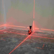
Удивительный мир нанотехнологии
Содержание:
- История
- Areas where nanotechnology is used
- Востребованность и значение нанотехнологииПравить
- Definition of nan’o•tech•nol’o•gy
- Do nanoproducts require special disposal?
- Top-down and bottom-up
- What is the real added value of nanotech?
- Nanotechnology in Electronics
- Why is nanotechnology important?
- How big is «nano»?
- Should nanoproducts be labelled?
- Nanotechnology in Energy
- Прогнозы и цифры развития НТПравить
- How do you work on the nanoscale?
- The future of nanotechnology: nanodream or nano-nightmare?
История
В 2000 году Правительство России разработало и приняло программу «Военная наноэлектроника Вооружённых Сил Российской Федерации на период до 2010 года».
21 августа 2001 года принята Федеральная целевая научно-техническая программа «Исследования и разработки по приоритетным направлениям развития науки и техники на 2002—2006 годы». 14 ноября 2002 года постановлением Правительства России в эту программу были добавлены разделы, связанные с нанотехнологиями и нанонаукой.
6 июля 2006 года принята Федеральная целевая программа «Исследования и разработки по приоритетным направлениям развития научно-технологического комплекса России на 2007—2012 годы», после чего финансирование по направлениям нанотехнологий и нанонауки возросло.
26 апреля 2007 года В. В. Путин в послании Федеральному Собранию назвал нанотехнологии «наиболее приоритетным направлением развития науки и техники». По мнению Путина, для большинства россиян нанотехнологии сегодня — «некая абстракция вроде атомной энергии в 30-е годы».
4 мая 2008 года Правительство России приняло «Программу развития наноиндустрии в Российской Федерации до 2015 года», согласно которой объём производства продукции наноиндустрии в России должен составить к 2015 году более 900 млрд руб.
8 октября 2008 года создано «Нанотехнологическое общество России», в задачи которого входит «просвещение российского общества в области нанотехнологий и формирование благоприятного общественного мнения в пользу нанотехнологического развития страны»
6 октября 2009 года президент России Д. А. Медведев на открытии Международного форума по нанотехнологиям в Москве заявил: «Все мы должны сделать так, чтобы нанотехнологии стали одной из мощнейших отраслей экономики. Именно к такому сценарию развития я вас призываю». Д. А. Медведев предложил Минобрнауки увеличить количество специальностей в связи с развитием потребности в квалифицированных кадрах для нанотехнологий.
26 апреля 2010 года в городе Рыбинске открылся завод по производству монолитного твёрдосплавного инструмента с многослойным наноструктурированным покрытием. Это первое нанотехнологическое производство в России. Роснано потратила на финансирование этого проекта около 500 млн рублей. Глава российского научного центра «Курчатовский институт» М. В. Ковальчук заявил: «Роснано в Рыбинском проекте сыграла очень важную роль в цепочке между научной организацией, финансирующим органом и конечным производством. Мы за бюджетные деньги создали интеллектуальную собственность, а затем с помощью Роснано коммерциализовали её и легально продали производственникам лицензию на её использование. Таким образом, благодаря этой госкорпорации наша технология была превращена в коммерческий продукт».
Areas where nanotechnology is used
Today, a life without nanotechnology is hard to imagine. Nanotechnologies – to be more specific: nanomaterials – are already used in numerous products and industrial applications. Our Nanotechnology Products and Applications database already provides an overview of how nanomaterials and nanostructuring applications are used today in industrial and commercial appplications across industries (please note: This is NOT a consumer products database that you can find elsewhere; so no antibacterial socks, bathroom cleaners, face creams, or pet products here…).
Our section «Ten things you should know about nanotechnology» provides you with an excellent first overview of what nanotechnologies are, what they are used for, and what some of the key issues are. If you want to get a more in-depth view of nanotechnology in important industry areas, then this section is for you. Also check out our primer How does nanotechnology work?
Here is a brief overview of some current applications of nanomaterials. Most of them represent evolutionary developments of existing technologies: for example, the reduction in size of electronics devices. They also give us an idea where nanotechnology will take us and where nanotechnology can be used in the future.
Востребованность и значение нанотехнологииПравить
На 21 августа, 2008, согласно проекту на новые НТ оценивается более чем в 800 идентифицированных изготовителями нанотехнологических продуктов, которые достижими с новыми качествами, удивляющими рынок в темпе 3-4 новых вида нанопродукто в неделю. Большинство заявок ограничено использованием первого поколения пассивных наноматериалов, которые включют:
- диоксид титана в солнцезащитный крем;
- косметику и немного продовольственных продуктов;
- углерод allotropes имел обыкновение производить ленту геккона;
- серебро в упаковке пищи, одежде, дезинфицирующих средствах и бытовой технике;
- цинковая окись в солнцезащитных кремах и косметике, поверхностных покрытиях, красках и наружных лаков мебели; и др.
Дальнейшие заявки, которые требуют соглосования и договоренности о видах компонентов. Их ждут далльнейшие исследования.
Например, следует назвать полученный продукт как Нано-мембраны, которые являются портативными и легко-очищаемыми системами, очищающие, детоксифицирующие и опресняющие воду. Это означает, что страны третьего мира смогли получить чистую воду, решая много связанных с водой проблем здоровья (цитата необходимая).
Или нанотехнология в оптике, когда наносреда из электромагнитно-двойных пар золотых точек в линзах вызывает новый эффект прохождения электромагнитных волн, например, в нанооптике.
НанооптикаПравить
Наносреда из электромагнитно-двойных пар золотых точек
электромагнитных волннанометрическомТГц12Гццветовплазменногооптикеоптической системы
Definition of nan’o•tech•nol’o•gy
So what exactly is nanotechnology? One of the problems facing this technology is the confusion about how to define nanotechnology. Most revolve around the study and control of phenomena and materials at length scales below 100 nm and quite often they make a comparison with a human hair, which is about 80,000 nm wide.
Some definitions include a reference to molecular nanotechnology systems and devices and ‘purists’ argue that any definition needs to include a reference to «functional systems». The inaugural issue of Nature Nanotechnology asked 13 researchers from different areas what nanotechnology means to them and the responses, from enthusiastic to sceptical, reflect a variety of perspectives.
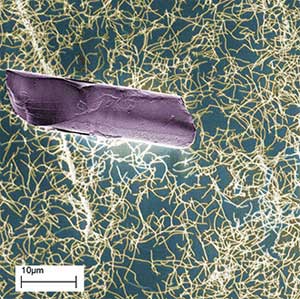
Human hair fragment and a network of single-walled carbon nanotubes (Image: Jirka Cech)
It seems that a size limitation to the 1-100 nm range, the area where size-dependant quantum effects come to bear, would exclude numerous materials and devices, especially in the pharmaceutical area, and some experts caution against a rigid definition based on a sub-100 nm size.
Another important criteria for the definition is the requirement that the nano-structure is man-made, i.e. a synthetically produced nanoparticle or nanomaterial. Otherwise you would have to include every naturally formed biomolecule and material particle, in effect redefining much of chemistry and molecular biology as ‘nanotech.
The most important requirement for the nanotechnology definition is that the nano-structure has special properties that are exclusively due to its nanoscale proportions. This definition is based on the number of dimensions of a material, which are outside the nanoscale (<100 nm) range.
Accordingly, in zero-dimensional (0D) nanomaterials all the dimensions are measured within the nanoscale (no dimensions are larger than 100 nm); in two-dimensional nanomaterials (2D), two dimensions are outside the nanoscale; and in three-dimensional nanomaterials (3D) are materials that are not confined to the nanoscale in any dimension. This class can contain bulk powders, dispersions of nanoparticles, bundles of nanowires, and nanotubes as well as multi-nanolayers. Check our Frequently Asked Questions to get more details.
Do nanoproducts require special disposal?

Nano | nanowaste Photograph: Linzid Hunter
One of the concerns over the widespread use of nanotechnology is that tiny particles could escape from where they are intended to be used and end up polluting the wider environment.
This is not a problem confined to nanotechnology of course, and a number of chemicals that we know to be toxic are used in everyday products such as light bulbs and batteries. Consumers are asked to dispose of these products carefully, but there is no way to be sure that they will do so. And some escapes are impossible to prevent – for example, much of the mercury in the atmosphere comes from the cremation of dead people with dental fillings.
The effects of nanoparticles on the wider environment are largely unknown, so perhaps a cautious approach is the best one?
Everyday examplesFactories and research laboratories could release nanoparticles in their waste streams. Many international bodies are looking at ways in which accidental release of nanoparticles can be monitored and prevented.
Potential risksToxic particles could pollute the natural environment and kill wildlife.
Illustrations by Linzi Hunter
Topics
Top-down and bottom-up
Nanomaterials can be constructed by top down techniques, producing very small structures from larger pieces of material, for example by etching to create circuits on the surface of a silicon microchip.
They may also be constructed by bottom up techniques, atom by atom or molecule by molecule. One way of doing this is self-assembly, in which the atoms or molecules arrange themselves into a structure due to their natural properties. Crystals grown for the semiconductor industry provide an example of self assembly, as does chemical synthesis of large molecules.
A second way is to use tools to move each atom or molecule individually. Although this ‘positional assembly’ offers greater control over construction, it is currently very laborious and not suitable for industrial applications.
Check out our detailed article on how nanoparticles are made.
What is the real added value of nanotech?

Nano | nanosales Photograph: Linzid Hunter
Nanotechnology is such a broad term that it is difficult to generalise about the value it could bring. There will be clear social value, in the form of cleaner energy and improved medicines; and individual value in that nanotechnology used in sporting equipment, for example, would improve an individual’s performance. On the other hand, having hundreds of products that are anti-bacterial most likely will not bring many additional benefits to society.
Value, to a certain extent, is in the eye of the user of the technology. A patient who can benefit from one type of tiny particle injected into their bloodstream to test for heart disease and so avoid surgery, for example, would probably see more added value than an average tennis player who started playing with a racket made and improved by using nanomaterials. A mis-hit still goes into the net after all, nanotech racket or not.
Everyday examplesNanotechnology is being used as a marketing tag to sell everything from socks and t-shirts to sports equipment. The true benefit comes from the way it is used by the consumer.
Nanotechnology in Electronics
-
Researchers at the Royal Melbourne Institute of Technology
have demonstrated atomically-thin indium-tin oxide sheets
that may make touchscreens that are cost less to manufacture and
well as being flexible and comsumes less power. -
Researchers at Ames Laboratory have developed
split-ring resonators made of metamaterials that can
generate tera-hertz
frequency signals. -
Researchers at North Carolina State University have
developed sensors using silver
nanowires that may be useful in robots and prosthetics. The nanowire
sensors can measure strain and pressure, and are flexiable enough to
work over the range of motion required by prosthetics. -
Researchers at Georgia Tech have demonstrated
antennas made of graphene.
They are working toward antennas and transceivers that would require
very little power and allow communication between nanomachines. -
Researchers at ETH Zurich have demonstrated
an optical switch
that can be changed between ON and OFF states by moving a single
silver atom.
More about
Nanotechnology in Electronics
Why is nanotechnology important?
Nanotechnology improves existing industrial processes, materials and applications by scaling them down to the nanoscale in order to ultimately fully exploit the unique quantum and surface phenomena that matter exhibits at the nanoscale. This trend is driven by companies’ ongoing quest to improve existing products by creating smaller components and better performance materials, all at a lower cost.
A prime example of an industry where nanoscale manufacturing technologies are employed on a large scale and throughout is the semiconductor industry where device structures have reached the single nanometers scale. Your smartphone, smartwatch or tablet all are containing billions of transistors on a computer chip the size of a finger nail.
How big is «nano»?
We live on a scale of meters and kilometers
(thousands of meters), so it’s quite hard for us to imagine a world
that’s too small to see. You’ve probably looked at amazing photos in
science books of things like dust mites and flies photographed with
electron microscopes. These
powerful scientific instruments make
images that are microscopic, which means
on a scale millionths
of a meter wide. Nanoscopic involves shrinking things down to a whole
new level. Nano means «billionth», so a nanometer is one
billionth of a meter. In other words, the nanoscale is 1000
times smaller than the microscopic scale and a billion (1000 million)
times smaller than the world of meters that we live in.
Should nanoproducts be labelled?

Nano | Nano products Photograph: Linzid Hunter
In November 2009, the European Union passed a law that will soon force manufacturers of cosmetics to state on the label if their products contain nanoparticles. Will more products follow? The issue of labelling has divided campaigners and politicians, just as it has with whether foods should be labelled as containing genetically modified ingredients.
Supporters of labels on nanotech say they will encourage consumer choice. Opponents say they will be meaningless without extra information on whether the nano-ingredients pose any risk. Without context, such labels could be misinterpreted as warnings, they say.
Everyday examplesLipsticks and face creams that contain nanoparticles will soon be labelled as such. Perhaps «nano-free» could then start to appear on products too?
Potential risksLabels might be a shortcut for industry to appear «transparent» without really informing the public.
Nanotechnology in Energy
-
Researchers at University of Massachusetts Amherst
have developed
protein nanowires that produce electric current when exposed to
water vapor in air. -
Researchers at Rice University are using carbon nanotube films to stop the growth of dendrites on lithium metal anodes. This step may help develop
lithium metal batteries, which could have much higher capacity and faster charging than lithium ion batteries. -
Researchers at UC Berkeley are working on a catalyst
consisting of
thin
sheets of metal carbide (instead of expensive
platinum) for the generation of hydrogen from water. -
Researchers at Berkeley Lab have
demonstrated that the combination of
magnesium
nanocrystals and graphene may be useful in storing
hydrogen for use in fuel cells. -
Researchers at Rice University have
performed computational studies that suggest that layers
ofgraphene separated by pillars of boron nitrate nanotubes
could be used to store hydrogen in cars.Researchers at Berkely Lab have have
developed a type of Metal-Organic-Frameworks
(MOFs) that has the
abilility to
store natural gas. The researchers believe this
material could be used to improve natural gas storage
tanks for vehicles and allow wider use of natural gas to
fuel cars.Researchers at the University of
Houston have demonstrated the use ofcobalt oxide nanoparticles as a photocatalyst to
produce hydrogen and oxygen gas from water using visible
light. More work needs to be done, both to increase the
energy efficiency and the lifespan of the nanoparticles,
before this catalyst is commercially feasible. -
Researchers at MIT have shown that
iron oxide nanoparticles in water can be used to
increase the amount ofheat transfer out of a system at localized hot spots.
The researchers believe this technique could be applied
to cooling a wide range of devices, from electronics
devices to fusion reactors.
More aboutNanotechnology in Energy
Прогнозы и цифры развития НТПравить
| Обзор прогнозов и цифр развития НТ | ||
|---|---|---|
| Объём продаж на мировом рынке (год) | Вид продукта | Источник информации |
| 493 млн. долларов США (2000)
900 млн. долларов США (2005) |
Неорганические наночвстицы и порошки (SiO2,TiO2,металлы, и т.д.) | 1)-BCC (2002) |
| 40 млрд.долларов
США (2002) |
Синтетические наночастицы как полуфабрикаты | 2)-BASF (2002) |
| 23 млрд.долларов
США (2003) 73 млрд.долларов |
Наноматериалы
Инструменты:компоненты нанотехнологии |
3)-Deutsche Bank
(2003) |
| 54 млрд. евро (2001)
100 млрд. евро (2005) |
НТ продукты (по убывающей): наноматериалы,
нанослои, наноаналитические препараты, |
4)-VDI,
5)-DG Bank(2001) |
| 66 млрд. долларов
США (2005) 148 млрд. долларов |
НТ продукты | Mitsubishi
Research 6)-(2002) |
| до 200 млрд. евро
(2005) |
НТ продукты | Sal. Oppenheim
7)-(2001) |
| 225 млрд. долларов
США (2005) 700 млрд. долларов |
НТ продукты | NanoBusiness
Alliance 8)(2001) |
| 1 триллион долларов
США (2015) |
НТ продукты вообще | 8)NSF (2001) |
How do you work on the nanoscale?
Your fingers are millions of nanometers long, so
it’s no good trying to pick up atoms and molecules and move them
around with your bare hands. That would be like trying to eat your
dinner with a fork 300 km (186 miles) long! Amazingly, scientists
have developed electron microscopes
that allow us to «see» things on the
nanoscale and also manipulate them. They’re called atomic force
microscopes (AFMs), scanning probe microscopes (SPMs), and scanning
tunneling microscopes (STMs).
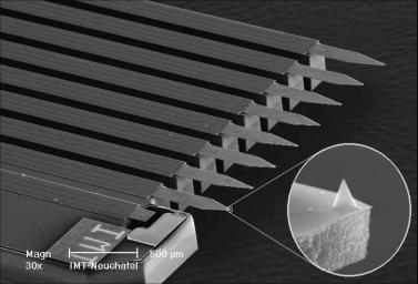
Photo: The eight tiny probe tips on the
Atomic Force Microscope (AFM) built into NASA’s Phoenix Mars Lander.
The tip enlarged in the circle is the same size as a smoke particle at its base (2 microns).
Photo by courtesy of NASA/JPL-Caltech/University of Arizona/University of Neuchatel.
The basic idea of an electron microscope is to use
a beam of electrons to see things that are too small to see using a
beam of light. A nanoscopic microscope uses electronic and quantum
effects to see things that are even smaller. It also has a tiny probe
on it that can be used to shift atoms and molecules around and
rearrange them like tiny building blocks. In 1989, IBM researcher Don
Eigler used a microscope like this to spell out the word I-B-M by
moving individual atoms into position. Other scientists have used
similar techniques to draw pictures of nanoscopic guitars, books, and
all kinds of other things. These are mostly frivolous exercises,
designed to wow people with nanopower. But they also have important
practical applications. There are lots of other ways of
working with nanotechnology, including molecular beam epitaxy,
which is a way of growing single crystals one layer of atoms at a time.
The future of nanotechnology: nanodream or nano-nightmare?
Engineers the world over are raving about
nanotechnology. This is what scientists at one of America’s premier
research institutions, the Los Alamos National Laboratory, have to
say: «The new concepts of nanotechnology are so
broad and
pervasive, that they will influence every area of technology and
science, in ways that are surely unpredictable…. The total societal
impact of nanotechnology is expected to be greater than the combined
influences that the silicon integrated circuit, medical imaging,
computer-aided engineering, and man-made polymers have had in this
century.» That’s a pretty amazing claim: 21st-century
nanotechnology will be more important than all the greatest
technologies of the 20th century put together!
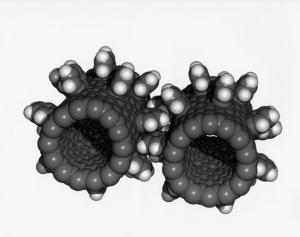
Photo: These nanogears were made by attaching
benzene molecules (outer white blobs) to the outsides of carbon
nanotubes (inner gray rings). Image by NASA Ames Research Center courtesy of
Internet Archive.
Nanotechnology sounds like a world of great
promise, but there are controversial issues too that must be
considered and resolved. Some people have raised concerns that
nanoscale organisms or machines could harm human life or the
environment. One problem is that tiny particles can be extremely
toxic to the human body. No-one really knows what harmful effect new
nanomaterials or substances could have. Chemical pesticides were not
considered harmful when they were first used in the early decades of
the 20th century; it wasn’t until the 1960s and 1970s
that their potentially harmful effects were properly understood.
Could the same happen with nanotechnology?
The ultimate nano-nightmare, the problem of «gray
goo,» was first highlighted by Eric Drexler. What happens if
well-meaning humans create nanobots that run riot through the
biosphere, gobbling up all living things and leaving behind nothing
but a chewed-up mass of «gray goo»? Drexler
later backed away from that claim. But critics of nanotechnology
still argue humans shouldn’t meddle with worlds they don’t understand,
but if we took that argument to its logical conclusion, we’d have
no inventions at all—no medicines, no transportation, no
agriculture, and no education—and we’d still be living in the
Stone Age. The real question is whether the promise of nanotechnology
is greater than any potential risks that go with it. And that will
determine whether our nano-future becomes dream—or
nightmare.


 Adblock